It is my honor to have this opportunity to share with you the analysis of the flash memory industry and the research and development of the chip, including some thoughts and explorations on the technological route of chip development.
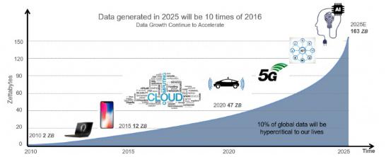
Data changes every day, but what's more important is how to analyze the data and derive value from it. Data is collected and analyzed, and the data is stored. The process of analysis requires a lot of storage. Therefore, the storage requirements will continue to grow and the demand will be very large. It will be a very big motivation and opportunity for the flash memory industry.
The traditional flash memory technology is called 2D flash memory. Today its development is hindered by its proximity to process limits. In this context, 3D NAND flash comes into being.
What is 3D NAND flash?
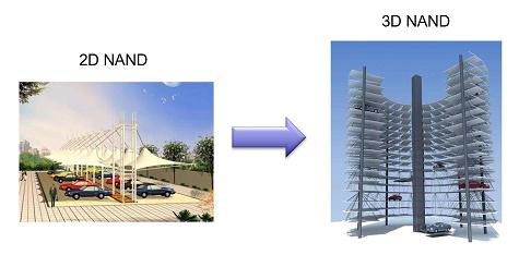
If we build a two-dimensional parking lot, our goal is to park as many cars as possible. But when the area is getting smaller, the space for each car is gradually compressed. Correspond to 3D NAND, the two-dimensional parking lot is moved in three-dimensional direction, which provides a new development direction for flash storage density. Not only do we have a larger room, but the position occupied by the car is relatively loose.
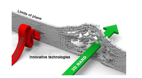
We are often asked the question: How long is your 3D NAND flash memory? This question is actually derived from the traditional concept of 2D flash memory. When they are 15 to 16 nanometers, the two-dimensional structure has reached a limit. There is no way in the industry to successfully increase density and keep cost down through the reduction of the two-dimensional structure. So 3D NAND flash memory is actually giving two-dimensional flash memory a new direction of development.
But the biggest advantage of 3D NAND flash is the increased density of flash memory and the continued cost reduction, which is helping people make better use of the data storage. Now 80% of the flash memory in the industry is 3D NAND.
The main 3D NAND flash memory is 64-layer this year, and everyone has heard some news about the 96-layer 3D NAND flash memory has appeared.
YMTC started our 3D NAND flash research and development in this environment. Since 2014, through the cooperation with the Chinese Academy of Sciences, YMTC’s management recognized the development opportunities of 3D NAND flash memory and started the investment and R&D of flash memory.
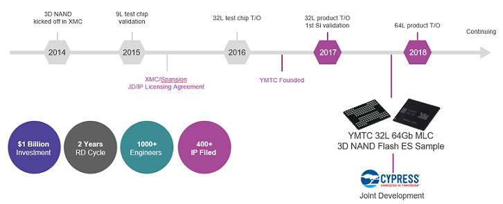
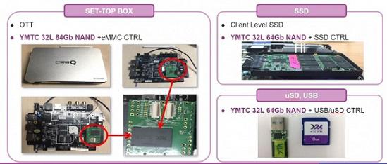
This year, we will continue to develop higher levels of flash memory, and our factories are also being built. This is the first flash application we successfully demonstrated last year. We're also thinking about how we can reduce the R&D cycle and bring the most advanced flash technology to the market. So these are the key points that we've been explored over the last two years.
Finally, let me talk about the three principles of YMTC. The most important thing for our flash memory and chip business is technology and innovation. Our competitors are very powerful, and their success is also based on their technological innovation. It is impossible to survive in this industry if there is no technological innovation. So it is our most important first step to continue to invest, and to have our own technology and intellectual property rights at our disposal.
Second, our goal is to be a profitable industry and a profitable enterprise. Only by making profits can we continue to invest in our technological innovation, and it is also possible to create benefits for our employees and society and shareholders.
Third, the semiconductor industry is a global industry. YMTC has some accumulation in the research and development of flash memory. But what we need more is the support from the global ecosystem of partners, so that we can make this enterprise and this industry bigger and better together to provide more value for society.
(This article is based on the keynote speech at the Storage Semiconductor Summit in 2018 of Dr. Yang Yuwen, Vice President of YMTC, which has not been reviewed by him.)